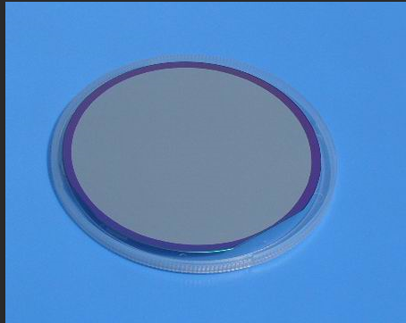
Silicon-On-Insulator(SOI) wafers
WaferHome can manufacture the IC Grade(等级) Silicon-On-Insulator(SOI) wafers


Specification for Silicon-On-Insulator(SOI) Wafer
| All over wafer | device layer | Buried oxided layer | Handle layer | ||||||
|---|---|---|---|---|---|---|---|---|---|
| Grade | Resisitivity | Geometric Parameter | Diameter |
Type/dopant |
Orientaion |
Thickness |
Thickness |
Orientaion |
Surface/Roughness |
| Bonding SOI Wafers | Customization | TTV < 5um Bow< 40um warp <40um | 25.4mm 50.8mm 76.5mm | P(Boron) N(Phos/As/Sb) | <100> <111> or special orientation |
1-30+/-1um customization | 0.1-7um |
<100> <111> or special orientation |
polished/polished |
| Customization | TTV < 5um Bow< 40um warp <40um | 100mm 125mm | P(Boron) N(Phos/As/Sb) | <100> <111> or special orientation | 1-30um customization | 0.1-7um | <100> <111> or special orientation | polished/etched polished/polished | |
| Customization | TTV < 5um Bow< 40um warp <40um | 150mm | P(Boron) N(Phos/As/Sb) | <100> <111> or special orientation | 1-30um customization | 0.1-7um | <100> <111> or special orientation | polished/etched polished/polished | |
| Customization | TTV < 5um Bow< 40um warp <40um | 200mm 300mm |
P(Boron) N(Phos/As/Sb) | <100> <111> or special orientation | 1-30um customization | 0.1-7um | <100> <111> or special orientation | polished/etched polished/polished | |
| Thin Device SOI Wafers | customization | TTV < 5um Bow< 20um Warp <20um | 25.4mm 50.8mm 76.5mm | P(Boron) N(Phos/As/Sb) | <100> <111> or special orientation |
10-500nm | 0.1-7um |
<100> <111> or special orientation |
polished/etched polished/polished |
| customization | TTV < 5um Bow< 20um Warp <20um | 100mm 125mm 150mm | P(Boron) N(Phos/As/Sb) | <100> <111> or special orientation | 10-500nm | 0.1-7um | <100> <111> or special orientation | polished/etched polished/polished | |
| customization | TTV < 5um Bow< 20um Warp <20um | 200mm | P(Boron) N(Phos/As/Sb) | <100> <111> or special orientation | 10-500nm | 0.1-7um | <100> <111> or special orientation | polished/etched polished/polished | |
| customization | TTV < 5um Bow< 20um Warp <20um | 300mm | P(Boron) N(Phos/As/Sb) | <100> <111> or special orientation | 10-500nm | 0.1-7um | <100> <111> or special orientation | polished/etched polished/polished | |
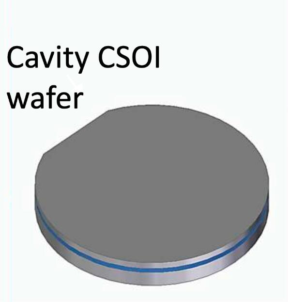
| Cavity SOI Wafer (CSOI) | customization | TTV < 5um Bow< 40um warp <40um | 25.4mm 50.8mm 76.5mm | P(Boron) N(Phos/As/Sb) | <100> <111> or special orientation |
customization |
|
<100> <111> or special orientation |
polished/etched polished/polished |
| customization | TTV < 5um Bow< 40um warp <40um | 100mm 125mm 150mm | P(Boron) N(Phos/As/Sb) | <100> <111> or special orientation | customization | <100> <111> or special orientation | polished/etched polished/polished | ||
| customization | TTV < 5um Bow< 40um warp <40um | 200mm | P(Boron) N(Phos/As/Sb) | <100> <111> or special orientation | customization | <100> <111> or special orientation | polished/etched polished/polished | ||
| customization | TTV < 5um Bow< 40um warp <40um | 300mm | P(Boron) N(Phos/As/Sb) | <100> <111> or special orientation | customization | <100> <111> or special orientation | polished/etched polished/polished | ||
| Silicon On Silicon | customization | TTV < 5um Bow< 20um Warp <20um | 25.4mm 50.8mm 76.5mm | P(Boron) N(Phos/As/Sb) | <100> <111> or special orientation |
customization | <100> <111> or special orientation |
polished/etched polished/polished | |
| customization | TTV < 5um Bow< 20um Warp <20um | 100mm 125mm 150mm | P(Boron) N(Phos/As/Sb) | <100> <111> or special orientation | customization | <100> <111> or special orientation | polished/etched polished/polished | ||
| customization | TTV < 5um Bow< 20um Warp <20um | 200mm | P(Boron) N(Phos/As/Sb) | <100> <111> or special orientation | customization | <100> <111> or special orientation | polished/etched polished/polished | ||
| customization | TTV < 5um Bow< 20um Warp <20um | 300mm | P(Boron) N(Phos/As/Sb) | <100> <111> or special orientation | customization | <100> <111> or special orientation | polished/etched polished/polished | ||
| Silicon-on-Glass(SOG) | customization | 100mm 125mm 150mm | 1 - 300um | ||||||
| customization | 100mm 125mm 150mm | 20 -1500nm | |||||||
| Gemanium-on-Insulator(GeOI) | customization | 100mm 125mm 150mm | 1 - 300um | ||||||
| 200mm | 20 -1500nm | ||||||||
| 300mm | customization | ||||||||
| Sappire on Silicon(SOS) | customization | 25.4mm 50.8mm 76.5mm | 1 - 300um | ||||||
| 100mm 125mm 150mm | 20 -1500nm | ||||||||
| 200mm 300mm | customization | ||||||||
| Sappire on Glass(SOG) | customization | 100mm 125mm 150mm | 1 - 300um | ||||||
| customization | 200mm 300mm | 20 -1500nm | |||||||
| LiNbO3 On Insulator(LNOI) | customization | 100mm 125mm 150mm | 1 - 300um | ||||||
| customization | 200mm 300mm | 20 -1500nm | |||||||
| LiNbO3 On Insulator(LTOI) | customization | 100mm 125mm 150mm | 20 -1500nm | ||||||
| customization | 200mm 300mm | 20 -1500nm | |||||||
| LiTaO3 On Insulator(LTOI) | customization | 100mm 125mm 150mm | 1 - 300um | ||||||
| customization | 200mm 300mm | 20 -1500nm | |||||||
| SiC On Insulator(SiCOI) | customization | 100mm 125mm 150mm | 1 - 300um | ||||||
| customization | 200mm 300mm | 20 -1500nm | |||||||
| SiC On SiC(Monocrystal) SiC On SiC(3C) |
customization | 100mm 125mm 150mm | 1 - 300um | ||||||
| customization | 200mm 300mm | 20 -1500nm | 3C | ||||||
| Silicon On SiC |
customization | 100mm 125mm 150mm | 1 - 300um | ||||||
| customization | 200mm 300mm | 20 -1500nm | |||||||

